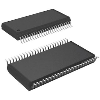
XC3S400-4PQ208I Field Programmable Gate Arrays
Field Programmable Gate Arrays (FPGAs) are
integrated circuits that are in demand due to their advanced features. The
field programmable feature of the device is enabling the programmers to
reconfigure the hardware according to the application requirements. For remote
deployment, the up-gradation of the features and debugging is a key
requirement. The FPGA technology is fulfilling all requirements.
The XC3S400-4PQ208I
belongs to the Spartan-3 family of Field-Programmable Gate Arrays. The module
XC3S400-4PQ208I is particularly designed to fulfill the needs of bulky and
cost-sensitive consumer electronic applications. The XC3S400-4PQ208I
builds on the successful launch and customer review on the earlier FPGAs by
modifying the previous designs. Modifications are performed by increasing the
total number of I/Os, the capacity of internal RAM, the number of logic
resources, and the overall level of performance. The module is not just
improving the previous areas but also improving the clock management functionality.
The XC3S400-4PQ208I is significantly enhanced using the cutting-edge features
derived from the Virtex-II platform technology.
Five programmable functional elements are building
the architecture of module XC3S400-4PQ208I.
The first element is referred to as the Configurable Logic Blocks (CLBs) that
comprise of RAM-based Look-Up Tables (LUTs) to aid in the implementation of
logical operations and storage elements. The alternative is seen as flip-flops,
registers, or latches. The second block is the Input/Output Blocks (IOBs) that
can control the data flow between the I/O pins and the internal logic circuits
of the module XC3S400-4PQ208I.
The third block is the Block RAM that ensures the provision of data storage
with the aid of 18-Kbit dual-port blocks. The fourth block is the Multiplier
block capable of accepting the two 18-bit binary numbers from the input pins
and perform the product calculation. The last block is A Digital Clock Manager
(DCM) block that facilitates the module with the feature of self-calibration,
and entirely digital solutions for, delaying, dividing, distributing,
multiplying, and phase shifting clock signals.
For the best delivery in terms of
cost-effectiveness of functionality and bandwidth, the enhancement of the
XC3S400-4PQ208I is done by combining it with advanced process technology. The
novel design approach is better than the previous designs and is setting new
standards and offering new challenges in the programmable logic industry.
Compared with different alternatives available in
the market, the XC3S400-4PQ208I is a better alternative for masking programmed
ASICs.The cost implication for previous approaches also compensates the FPGA
due to the reduction in the high initial cost. The complexity is also lowered
due to avoidance of the lengthy development cycles, and the inherent
inflexibility of conventional ASICs. Also, the programming feature of the FPGA
allows the design to perform up-gradation without the requirement of any
hardware replacement. This is not the case with the ASICs and making the FPGAs
superior to previous approaches,
A few distinct features of the XC3S400-4PQ208I include:
- Densities that are up to 74,880 logic cells
- Clock skew elimination
- Abundant logic cells with shift register capability
- Signal swing ranging from 1.14V to 3.465V
- High-resolution phase shifting
- Termination by Digitally Controlled Impedance
- 18 single-ended signal standards
- DDR, DDR2 SDRAM support up to 333 Mb/s
- 8 differential I/O standards including LVDS
- RSDS, Double Data Rate (DDR) support
- Logic resources
- Frequency synthesis
The features and characteristics of the XC3S400-4PQ208I added to the exceptionally low cost make the XC3S400-4PQ208I suitable for a wide range of consumer electronics applications, including access at the broadband level, digital television equipment, home networking, and, display/projection.


Comments
Post a Comment